Introduction
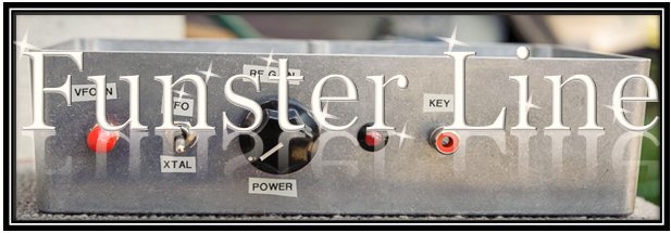
I began the Funster transceiver line in 1995 and show the 2014 version [now back to a CW trans-receiver on the 40M band]. Judging by reader feedback, plus analog scratch-homebrew threads in social networks, email lists and print, many of us feel a nostalgic pull towards old-school radio. Me too.
Now at version 8 — Funster shares my joy in making a simple, old-style radio with all discrete parts. In some ways, this radio set is a twisted version of Wes and Roger’s Ugly Weekender from QST for August 1981.
Summary
Variable power: 128 to 3312 mW @ 13.6 VDC. Switchable 7.04 MHz xtal oscillator or external VFO input port. Solid state transmit/receive [T/R] circuit with PIN diode. External continuous and switched 12 VDC power jacks. Single-ended BJT Class C power amplifier with 67% efficiency.
Note: I state 12 VDC in my DC circuits, however, this nominal value might better be termed 12 -13.6 VDC.
Key up power current draw @ 13.6 VDC = 17 mA. Key down current @ 3W RF power with 13.6 VDC = 420 mA.
DC Circuitry
It’s fun to march off the signal path and focus on DC circuitry — switching, regulating and filtering the DC voltage feeding our RF or AF stages with finesse. Trans-receivers contain DC, RF, AF and external patch cords that benefit from mindful DC line filtering + selective high-isolation amps in the signal path to prevent RF flowing where it’s unwanted. You’ll see heaps of decoupling with RF + AF bypass and a few strong reverse-isolation amplifiers in this radio set.
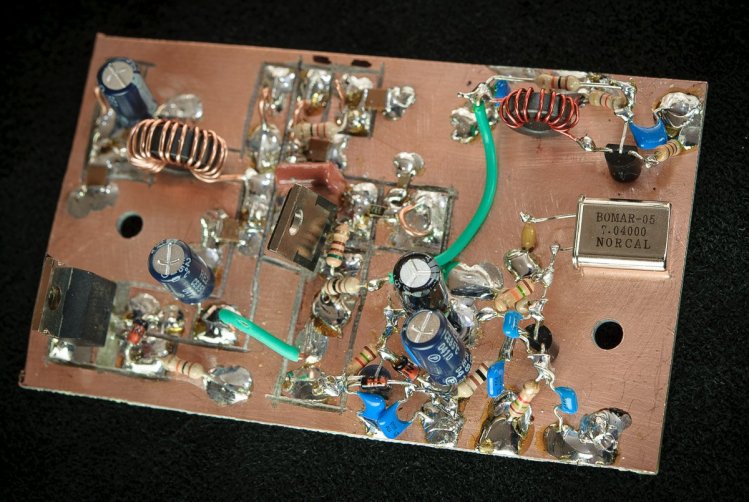
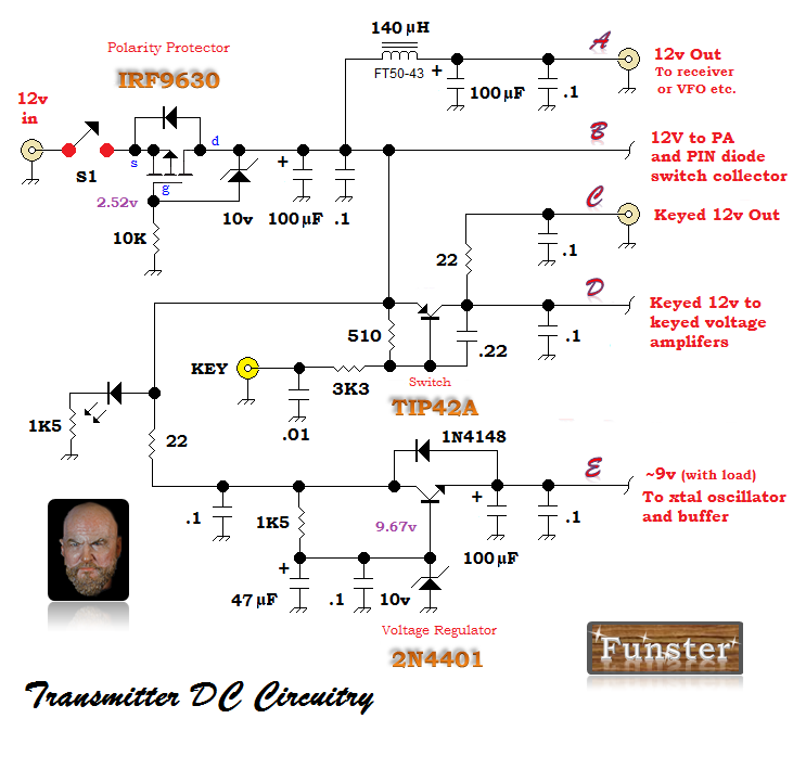 Above — The DC circuit board. A reader sent me 2 IRF9630 power MOSFETS: avoiding the voltage drop of the usual single rectifier diode, I employed 1 as a reverse polarity protector. Another reader sent me a long strip of 2N4401 BJTs, so I ran them instead of the equally good 2N3904. Thanks for the parts guys!
A simple series voltage regulator with a zener diode reference supplies DC to the crystal oscillator and its buffer. The base-emitter voltage drop of the 2N4401 emitter follower lays in series with the load, so load current changes alter the regulator output voltage. Vout = Vzener – VBE : so the regulated voltage is roughly 9 VDC.
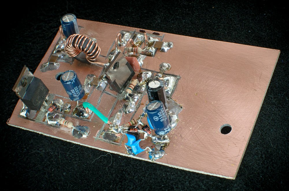 Above — DC circuitry breadboard photo.
Oscillator Circuitry
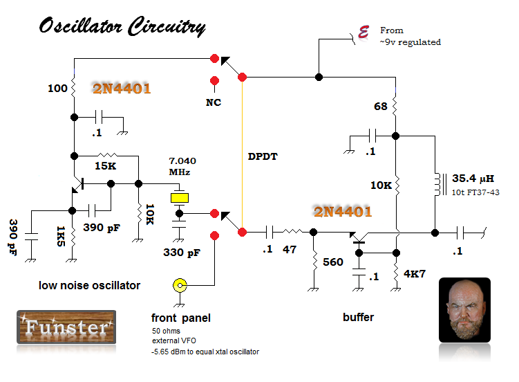 Above — Oscillator circuitry. I soldered my oscillator circuitry on the DC control board. To equilibrate to the xtal oscillator AC output voltage, the VFO input port should run about -5.65 dBm. I might stick a 6 dB attenuator pad on the front panel switch and use a 7 MHz VFO with 0 dBm output power.
 Above — Oscillator (and DC) circuit breadboard.
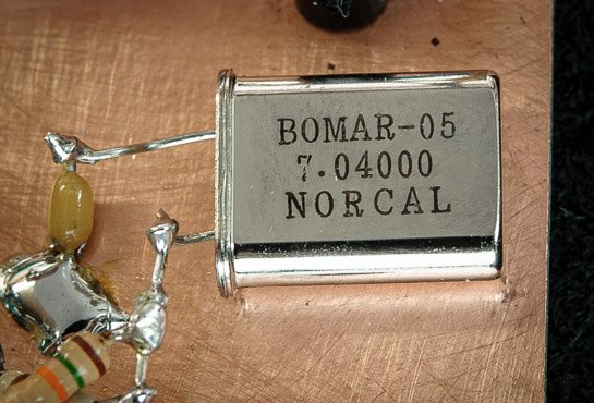 Above — Close-up of the old NorCal crystal supplied by NT7S — thanks Jason!
Keyed Voltage Amps
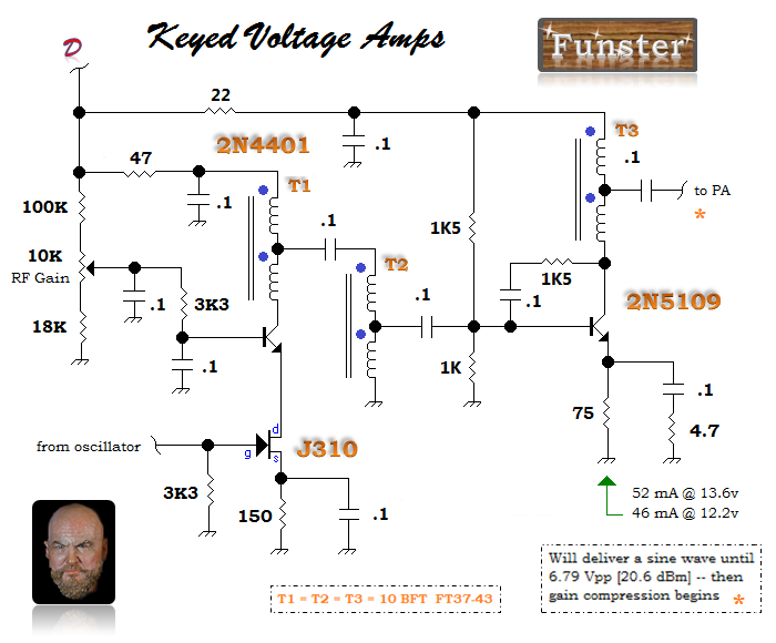 Above — The 2 keyed voltage amplifiers. I set the value of the RF gain pot series resistors by placing a 100K pot before and after the 10K gain pot and tweaked them back and forth to find close to 3W maximum and 125 mW minimum RF power with the gain pot set @ CW and CCW respectively. The 100K pots were removed, measured and nearest standard value resistors substituted: 100K and 18K.
By carefully choosing the 75 Ω emitter resistor, the 2N5109 feedback amp output remains a sine wave at the drive levels needed for a PA output at 3 Watts. At 3 Watts PA output, the feedback amp output voltage = 5.91 volts pk-pk [19.4 dBm]. The emitter current shown will cleanly drive a PA for more power if desired. Boost it as needed.
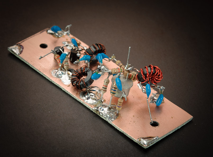 Above — AC voltage amps breadboard photograph.
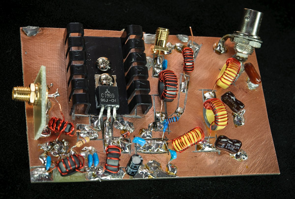
Power Transistor and T/R Switching
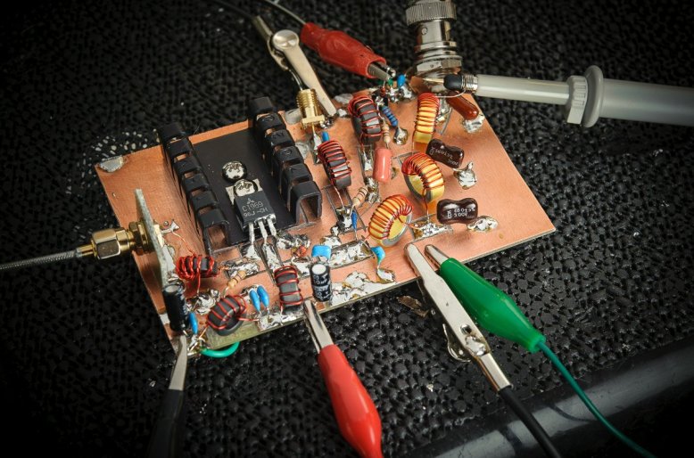 Above — Final testing the PA and T/R circuitry before installing it into the Hammond chassis.
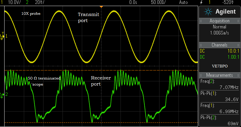
Three temporary RF connectors were soldered on this board for bench measurement. I connected the (SMA) receiver port to Channel 1 of my 50 Ω terminated ‘scope to measure the RF not getting shunted to ground by the PIN diode. The SMA cable/connector to the far left is a temporary cable connected to the keyed voltage amp board output in the Tx chassis — thus I tested the PA stage with its own xtal oscillator and RF amplifiers. The right-sided BNC RF port connects the PA low-pass filter to a 10W, 50 Ω dummy load via a 22 cm 50 Ω patch cable.
Further, I measured collector voltage + collector current with 2 DVMs and also PA output power in my oscilloscope (DSO) Channel 2 with a 10X probe employing a tiny ground lead.
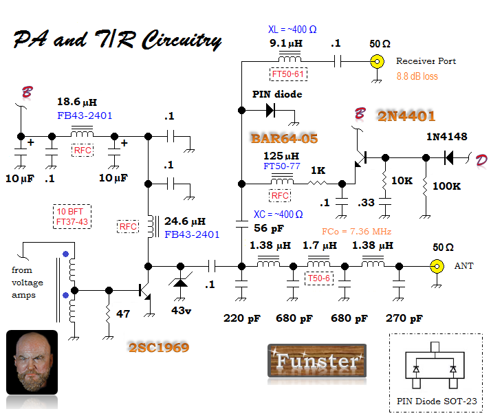
Above — PA and T/R circuitry schematic. Although we might run a BD139 or other cheap BJT for the final, I chose my favorite HF classic, the 2SC1969. This transistor will survive a high VSWR, however a 43 volt – 500 mW zener diode further protects it from such.
In 1 version with a 1:4 Z collector matching network and no zener diode, I measured 6.25W RF power after tweaking the 100K and 18K RF gain limiting resistors in the preceding hycas voltage amp to drive the PA harder. At ~3W maximum power in my final experiment, the 2SC1969 barely warms up.
Collector Matching
After a number of experiments, I learned that from tens of mW up to ~ 3.3 Watts RF power, we may omit collector matching and still get reasonable efficiency if you run a collector choke >= 15 μH. Thus, I made the maximum power ~ close to 3W — easy peasy.
Ask QRP enthusiasts what QRP is all about and they might extol the thrill of exacting the most kilometers per Watt — in keeping with that spirit, I love turning down my Tx power and the Funster front panel RF gain control makes it a breeze.
The PA circuit is standard fodder. I wound the 24.6 μH and 18.6 μH RFCs on FB43-2401 ferrites [a single hole bead that looks like a fat FT37-43]. An FT37-43 or FT50-43 makes a great substitute.
PA Measures
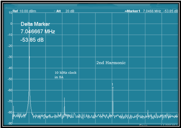 Above — Spectrum analysis of the Tx output. The 10 MHz clock signal from my spectrum analyzer lays between the fundamental and 2nd harmonic. The 2nd harmonic = -53.85 dBc @ 3W power output.
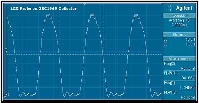 Above — PA collector waveform at 3W output measured with my DSO’s 10X probe.
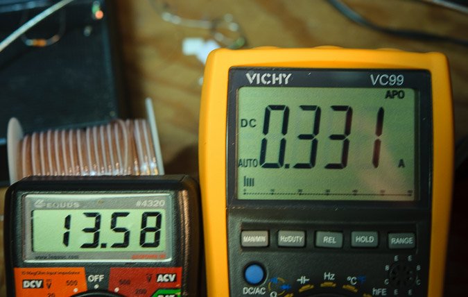 Above — Set your meters on stun! DC measures to calculate PA efficiency [See RF Workbench 6]: DC power = 13.58V x 0.331A = 4.49W. RF power = 3W. Efficiency = RF power / DC power = 3W / 4.49W = 66.8%.
T/R Discussion for Single Band Transceivers
Previous Funsters ran a simple QSK T/R circuit developed by Wes, W7ZOI in the early 1980s: a series X = 500 Ω resonator with anti-parallel diodes between the L and C. The series capacitor presents 500 Ω reactance to the 50 Ω transmit line so that only a small portion of the transmitter power flows to ground via the diodes and even less reaches the receiver input. In short, the 500 Ω capacitive reactance + clamping action of the anti-parallel diodes protect the receiver front end.
For 1 band, this simple circuit sizzles. Two potential concerns:
- ~6-9 dB loss of the receive signal making it better for lower HF, although I’ve seen builders add a receive preamp and use this T/R system on 12 and 10 meters. Since both band noise and signals get attenuated simultaneously, I’ve rarely had readability issues on 160-30 meters in my popcorn transceivers.
- The anti-parallel diodes may cause IMD. The intercept for the 500 Ohm series reactances with shunt diodes is around +6 or +7 dBm. This might exert problems in a high performance receiver front end, but poses a non-issue with typical NE612 front ends. Many builders, including Wes, reduce IMD potential with 2 or 3 series diodes on each leg. Another solution includes running a PIN diode as the shunt element. That’s what I did.
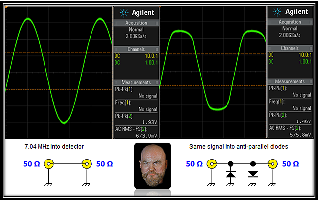 Above — The DSO tracing of an experiment showing the before and after effect of 2 anti-parallel diodes. The voltage across a silicon diode varies with the current going through it. Silicon diodes don’t conduct much current until the voltage across them reaches a threshold [ typically ~0.6 to 0.7 volts ].
In situ, the forward threshold voltage of each diode limits the circuit voltage by clipping off AC voltage above its threshold. Clamping refers to the limiting of voltage in 2 directions using anti-parallel pair(s) of clipping diodes. For example, if a negative-going AC dips more than 1 diode drop below ground, the left hand diode will begin to conduct and clip off any voltage above its threshold. This, of course, describes the “ideal diode” — in real life, factors like switching speed, current-handling and temperature are all in play.
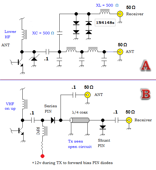 Above — 2 possible T/R schemes. Figure A shows the classic W7ZOI T/R system with 2 diodes per leg. See EMRFD Fig 2.112, for an example with 3 diodes per leg. For 1 band, it’s often our go-to circuit.
Figure B shows a scheme well suited for VHF on up: Both PIN diodes get forward biased during transmit mode, however, a 1/4 wave transmission line lays between the series and shunt PIN diode. 1/4 wave transmission lines exert magic [actually it’s pure physics that may be verified with a Smith chart].
When the shunt PIN diode gets biased on and grounds the receiver port end of the transmission line, the other end looks like an open circuit and thus power flows to the antenna port and not into the forward biased shunt PIN diode to ground. I hope to apply this system in future VHF and UHF projects and sadly, it’s impracticable at HF.
Funster Version 8 T/R Switching
As it happens, I seek experience with PIN diodes and therefore shunted a PIN diode instead of running anti-parallel diodes in the classic W7ZOI T/R scheme. This meant adding a transistor switch to quickly bias on the PIN diode @ key down and run a little hang time @ key up.
Please refer to the PA-T/R schematic. During key down, keyed 12 volts saturates the 2N4401 switch and 11 ma current biases on the PIN diode. At key up, the BJT switch’s base voltage is held on by the 10K plus series 0.33 μF capacitor just long enough to allow the stored energy in the large PA collector choke to collapse — protecting the receiver.
Feel free to experiment with the timing capacitor value.
Previously, Wes, W7ZOI suggested connecting the T/R receiver port to a 50 Ω terminated ‘scope for general measurement and also for clocking up RC time constants in DC switching circuits. With a 2 channel ‘scope you can monitor the receiver port switch function in 1 channel while watching the PA collector AC voltage in the other. Now that’s experimenting!
 Above — A 2 channel sample from my QRP workbench.
I chose an XC / XL of 400 Ω for the series L-C network. The 9.1 μH coil shouldn’t be wound on a 43 material ferrite [the Qu is just too low]: a bigger powdered iron toroid like size 68, or even a 61 ferrite material toroid works okay from my experiments [Q’s as high as 162 were measured on a FT50-61 @ 1 MHz in 2013]. Although this coil tunes coarsely, try tweaking the 9.1 μH inductor with thumb and forefinger during actual signal testing in a receiver.
I wound the 125 μH choke connected to the pin diode cathode on a 77 material ferrite toroid to get it done with just a few turns and avoid a self resonant frequency close to 7 MHz.
 Above — 50 Ω terminated DSO measurement of the receiver port @ 3W transmitter power. Theoretically all power should shunt to ground through the PIN diode, however, the diode exhibits a little resistance and the series L-C circuit contains reactance, so isolation is never perfect.
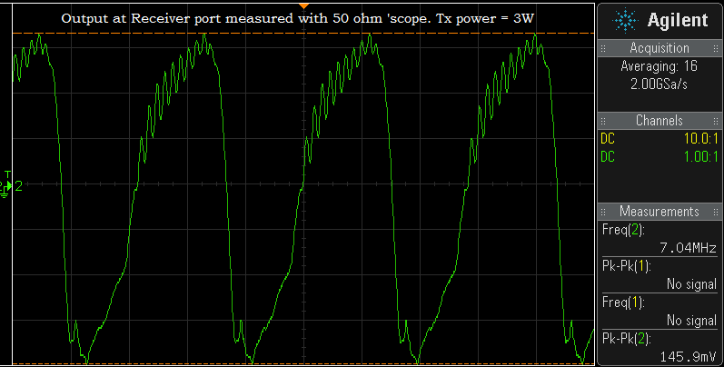
 Above — A low-pass filtered measure of the receiver port while in transmit mode. The beauty of a 50 Ω measurement environment shines: I placed a 7.36 MHz-bench module low-pass filter between the receive port and my DSO to quantify the leaked power to the receiver port as -14.17 dBm when the transmitter delivers 3W. Safe for my receiver.
My sincere thanks to those who offered advice and feedback during the build of this transmitter.
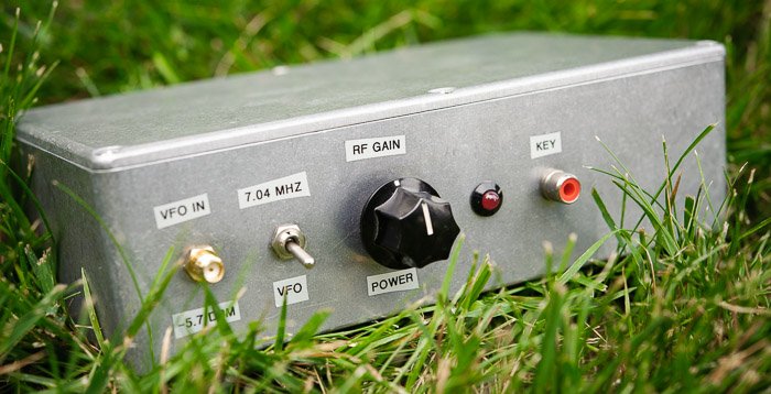 Above — Funster in the field.
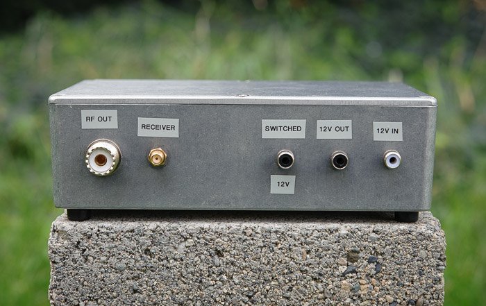 Above — Rear view of the Funster Tx.
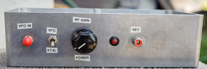 Above — Front view of the Funster Tx.
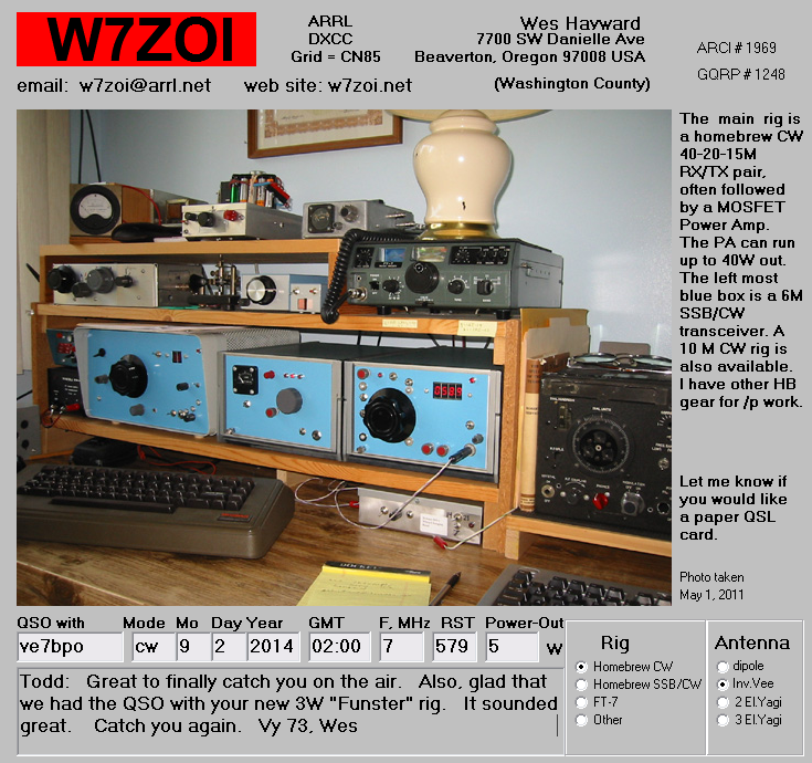
Above — First Funster QSO: Wes, W7ZOI and Bob, N7FKI
References
- Perfecting a QSK System. QEX for Mar/Apr 2006. Markus, VE7CA. Click for pdf.
- Electronic Switching and How it Works, QST for September 1984. Doug, W1FB.
- 7 MHz receiver — discussion begins on page 215 — On page 214 in Fig 1 see the 33 pF input cap plus receiver protecting anti-parallel diodes. Also view the 555 timer and other T/R control circuitry in Figure 2 on page 215.
This receiver realizes the first-ever printed version of the W7ZOI T/R system described earlier. Solid State Design for the Radio Amateur. ARRL,1986 [out of print] by Wes, W7ZOI and Doug W1FB.
- Transmit – Receive Antenna Switching. EMRFD. First published by the ARRL in 2003. Page 6.68.
- Schematic for the 30-W, 7 MHz power amplifier. Figure 2.112 [page 2-42] EMRFD. Design by Wes, W7ZOI


